The slides, written out
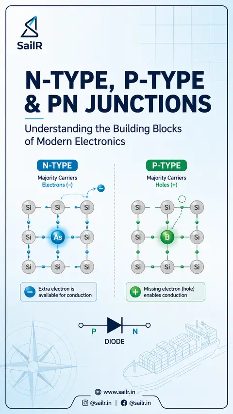
AI-drawn illustration. Simplified to explain the idea, not to scale.
Slide 1 · N-TYPE, P-TYPE
N-TYPE, P-TYPE
& PN JUNCTIONS
Understanding the Building Blocks
of Modern Electronics
N-TYPE
Majority Carriers
Electrons (−)
P-TYPE
Majority Carriers
Holes (+)
Extra electron is
available for conduction
Missing electron (hole)
enables conduction
P
N
DIODE
|
Slide 2 · 2/4
N-TYPE
SEMICONDUCTOR
Doped with pentavalent (donor) impurities
to create free electrons.
LATTICE STRUCTURE
PENTAVALENT DOPANTS
Arsenic (As)
Antimony (Sb)
Phosphorus (P)
KEY POINTS
Five valence electrons.
Four electrons form covalent bonds with neighbouring silicon atoms.
One electron is weakly bound to the donor atom and becomes free.
Electrons are the majority carriers.
Donor impurity material.
Si Silicon atom
As Pentavalent dopant (Arsenic)
Covalent bond
Free electron
CURRENT FLOW
When a voltage is applied, free electrons move toward the positive terminal (anode).
Electron flow
N-TYPE (−)
POSITIVE TERMINAL (ANODE)
|
Slide 3 · 3/4
P-TYPE
SEMICONDUCTOR
Doped with trivalent (acceptor) impurities
to create holes.
LATTICE STRUCTURE
TRIVALENT DOPANTS
Boron (B)
Aluminium (Al)
Gallium (Ga)
Indium (In)
KEY POINTS
Three valence electrons.
Forms only three bonds
with neighbouring silicon
atoms.
One bond remains incomplete,
creating a hole.
Holes are the majority
carriers.
Acceptor impurity material.
Si Silicon atom
B Trivalent dopant (Boron)
Covalent bond
Hole (missing electron)
CURRENT FLOW
Electrons from neighbouring atoms
move into the hole to fill the gap.
This leaves a new hole behind.
The hole appears to move in the
direction of conventional current
(positive to negative).
Hole movement
(conventional current)
Hole
Electron movement
|
Slide 4 · 4/4
THE PN JUNCTION
When N-type and P-type semiconductors are joined,
a PN junction is formed.
N-TYPE
(Electrons)
DEPLETION LAYER
(No free charge carriers)
P-TYPE
(Holes)
Free electron
Positive donor ion
Negative acceptor ion
Hole
A
FORWARD BIAS
(Conduction)
B
REVERSE BIAS
(Blocking)
Positive to P-side, Negative to N-side
Negative to P-side, Positive to N-side
External voltage reduces the barrier.
Depletion layer becomes thinner.
Electrons and holes cross the junction.
Current flows easily.
Typical silicon diode drop ≈ 0.6 – 0.7 V
External voltage increases the barrier.
Depletion layer becomes wider.
Electrons and holes are pulled away
from the junction.
Current is blocked.
Only a tiny leakage current flows until
breakdown voltage is reached.
The PN junction is the foundation of every
semiconductor diode, rectifier, transistor,
and integrated circuit.
A
(Anode)
K
(Cathode)
|
Drafted by SailR from our daily lessons. AI-drawn illustration. Simplified to explain the idea, not to scale. Last updated 19 Oct 2026.
Spotted a mistake?